
A new approach to detecting defects on PCBs that identify spatial location and extent is proposed, with potential applicability to similar manufacturing scenarios that use tiny components. We use a hierarchical multi-resolution approach to image analysis. The idea is that different levels of image resolution can provide different kinds of information about the target. Each such level can be processed at an acceptable resolution for deep learning, and we proceed deeper hierarchically, maintaining similar image resolutions where possible. The end result from such a hierarchical exploration can be synthesized for overall analysis. This enables the processing of very high-resolution images, which otherwise require extremely high computational time and cost investments for neural network training. We also present an approach that spatially locates defects (location, size, and shape) on PCBs using only unsupervised training with sane or good images. Extensions and further scope are discussed.
Introduction
Computer vision(CV) based Artificial intelligence methods (AI) have shown great success in detecting defective products in a manufacturing pipeline. Localization and characterizing spatial extents of those defects have been a challenge with the lack of availability of industry-specific data samples.
Printer Circuit Board (PCB) manufacturing pipeline addresses such challenges with Automated optical inspection (AOI) systems looking for open solder joints, missing components, misaligned components, wire breaks, bent pins, fluid leaks, shorts, and so on. For each of these, there is a whole class of defect types. With the publicly available datasets addressing common defects, detecting specific regions and defect type needs advanced and customized algorithms.
Approaches & Challenges
Common object detection models such as YOLO, SSD, R-CNN, and others can be trained to detect different types of defects on a PCB. Such models are expected to predict a bounding box on an input image where a specific defect is contained. Image segmentation models such as U-net, Mask R-CNN, and Deep Lab can be deployed with a transfer learning strategy for a specific instance of a defect. Obtaining exhaustive samples of defects is a challenge. Also, the requirement of a very high resolution of the images becomes a prime necessity owing to micro-level dimensions of components and defects. Large image sizes are harder to train on neural networks, with an equivalent rise in computational costs.
Combining Object detection & Autoencoders
A novel approach to detect and locate defects on a PCB, with a reduced number of training images and with lesser computational cost despite high-resolution images has been developed.
The approach comprises two stages in the inference pipeline. The first stage identifies various PCB components in a lower resolution which is downsampled. While PCB is identifiable, Faster R-CNN locates all components with very few images.
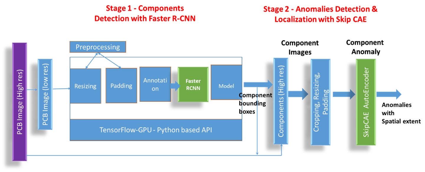
Fig 1. Inference Pipeline
In stage 2, we move to defect detection and localization of components. Bounding boxes of components from stage 1, are upscaled and used to extract components from high-resolution PCB images. These tiny, high-resolution component images become the input for Convolutional Auto-Encoder (CAE) with skip connections, similar to those used in U-Net for inference. These CAE algorithms are trained with normal component images and failure in reconstruction becomes an anomaly.
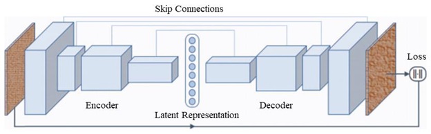
Fig 2. Convolutional AutoEncoder (CAE) with skip connections
The reconstruction loss is a parameterizable threshold. A heatmap of an XOR operation subtracting the input and the learnt CAE template images reveals the location and spatial extent of defects on the component. Some example images are given below.
Skip connections-based CAEs have been used and show good results. With the choices available, other CAEs could be used based on need and computational costs.
Results
We have uses a hierarchical multi-resolution approach to image analysis. The idea is that different levels of image resolution can provide different kinds of information about the target. Each such level can be processed at an acceptable resolution, and we proceed deeper hierarchically, maintaining similar image resolutions where possible. The end result from such a hierarchical exploration can be synthesized for overall analysis.
One prime difference with other approaches is that we have used only sane or good images of components to train CAEs for detecting defects. There is no reliance on any sort of large datasets that contain all possible defect types and shapes. Such datasets are also very hard to come by. The CAEs are able to accurately find the location, size, and shape of defects.
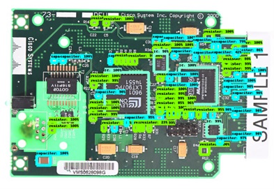
Faster R-CNN with Resnet-50 V1 Object detection model scaled for 1024 x 1024 resolution has been able to achieve results. Faster RCNN combined with Resnet known for its skip connections during the backward propagation has shown good success for tiny objects in remote sensing images. Resnet architectures are known for avoiding both vanishing and exploding gradient problems. Training of the model was done through use of component images from the FICS-PCB dataset which is recommended for classification models. The dataset includes full PCB images in addition to components. We found that our Faster R-CNN model did a good job of detecting ICs, resistors, capacitors, and other components.
 The autoencoders (one per component type) were trained with images of good components, i.e. without any defects on them. Without any labeling and classification, CAE learned to reproduce its input, test, and validation images with very little loss. After training, if images with defects are given to a trained CAE, reconstruction of those images will not be accurate. The actual defects on a component can be located by inspecting these reconstruction losses. In the examples below we also introduced synthetic defects on component images to see how the autoencoders perform.
Fig 3. Components detection on PCB
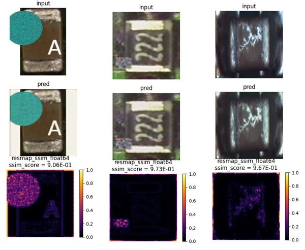
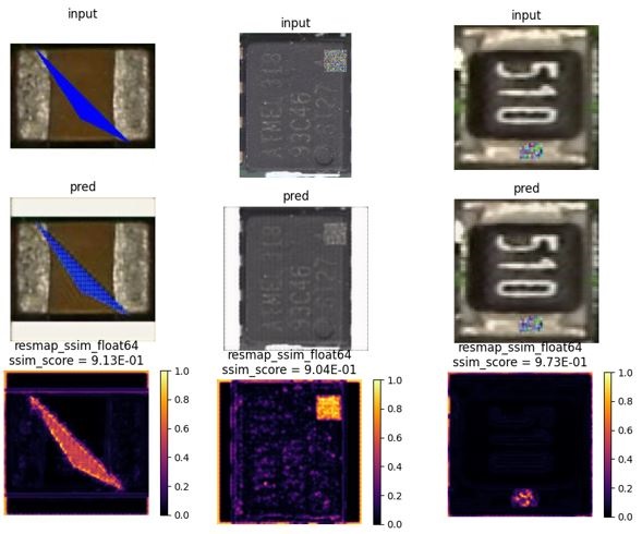
Fig 4. Heatmaps of synthetic defects introduced on PCB components
Going Further
Here are some straightforward extensions to increase the scope and accuracy of our approach, in addition to using larger datasets.
1. Missing Components: Object detection can provide a simple inventory count of the components on a given PCB image, to identify what specific components are missing if any, and from where. This can be done against a master inventory and template for the PCB.
2. PCB-specific Learning: One may also train the models mentioned above for specific PCBs being manufactured so that the accuracy of detection on those PCBs can be higher. This must be done through a transfer learning approach where a model originally trained on a larger data set and has learnt general features is then fine-tuned for a given PCB.
3. Classifying Defects: The heatmaps generated by the CAEs will have different shapes and sizes depending on the types of defects that were detected. An image classification model trained on these heatmaps may be used to also identify what kind of defects they represent (in technical terms).
4. Alignment Problems: Component alignment issues are not directly addressed by this approach. But the CAEs can also be trained to generate segmentation maps. A border/contour detection algorithm or template matching algorithm can be used to check if the segmented components are misaligned vs a master template. Another approach may use image subtraction, as is common.
5. Beyond Components: Nothing restricts a given CAE to be trained for just one component. CAEs can be trained with multiple components within a whole image perspective. This can be used to locate defects that occur in between components, especially when trained on a specific PCB (using transfer learning). Training CAEs on whole PCBs require large datasets and lots of computing time & power because of the high resolutions involved. One can always find a good middle ground between individual components and full PCB images.
6. 3D Inspection: 3D is another interesting area. The human neuronal network constructs 3D visualizations from 2D stereo images provided by the eyes. Note that a convolutional network takes an image volume (e.g. RGB planes) as input. Images from multiple fixed perspectives can be added to this volume, even in grayscale where possible. For a CAE, the losses or heatmaps generated for individual planes need to be combined into a 3D mapping to visualize the defects. There are several techniques and papers extant on using 2D images to create 3D visualizations.
7. Hierarchical multi-resolution: Even though we have used only 2 levels of image hierarchy in our analysis, one could very well define multiple levels between whole PCB images and individual components. This is left for future work.
Conclusions
We believe that the work presented here, though limited by a relatively small dataset, provides an approach of significant value in automating manufacturing QC flows. It also demonstrates a useful direction towards a robust and reliable image anomaly detection system for PCBs.